
1. 5G High-Frequency Device Design
2. 5G High-Frequency Materials
3. ANSYS-HFSS
4. Automotive Electronics
5. Synchrotron X-ray Microdiffraction
6. Nanotwined Cu
Doctoral Student: Cheng-Yu Lee
Master(Full Time): Jun-Chou Yu, Shun-Cheng Chang
Equipment: Cheng-Yu Lee
CSO: Jun-Chou Yu
Accounting Business: Shun-Cheng Chang
Business Network: Cheng-Yu Lee
Advanced Semiconductor Packages Materials Labaty (ASPML) was established by Dr. Cheng-En Ho in August, 2007. We direct our research activities at the development processing of microelectronic packaging technologies materials, specifically focusing on lead-free solders, interfacial reactions, electromigration, the growth of tin whiskers. The central theme of our research is solid-state diffusion, reaction kinetics, phase transformations in the metallic system. Currently, we are also working on the synchrotron radiation study in multiphase alloys under current stressing. This project is in cooperation with Dr. Ku (Beamline 21A) and Dr. Tseng (Beamline 23A) in National Synchrotron Radiation Research Center (NSRRC).
1. ANSYS HFSS
2. ANSYS Mechanical
3. COMSOL Multiphysics-RF Module
4. COMSOL Multiphysics-Electrodeposition Module
5. Polish Machine
6. Convectional Oven
7. Digital DC Power Supply
8. Ultrasonic Cleaner
9. Precision Cut-off Machine (Minitom)
10. Vibraty Polisher (Vibromet 2)
11. Probe Station
12. High-Speed Ball Shear Test
13. High-speed Plating Haring Cell
14. Optical Microscope
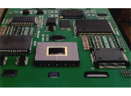 Microelectronic Packages
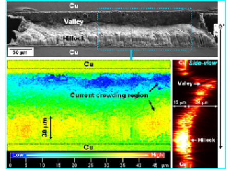 Electromigration
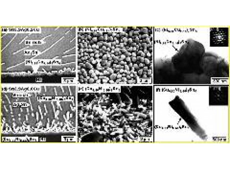 Lead-Free Soldering
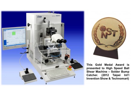 High Speed Ball Shear Test
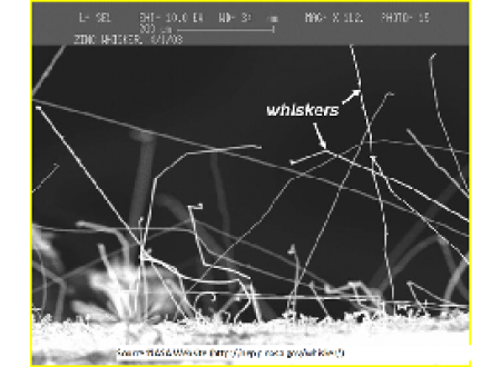 Tin Whiskers
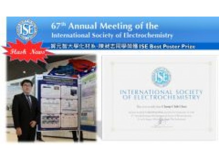 Best Poster Prize of 2016 ISE Annual Meeting
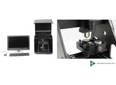 Nanoindenter (勀傑科技demo)